- English
- Español
- Português
- русский
- Français
- 日本語
- Deutsch
- tiếng Việt
- Italiano
- Nederlands
- ภาษาไทย
- Polski
- 한국어
- Svenska
- magyar
- Malay
- বাংলা ভাষার
- Dansk
- Suomi
- हिन्दी
- Pilipino
- Türkçe
- Gaeilge
- العربية
- Indonesia
- Norsk
- تمل
- český
- ελληνικά
- український
- Javanese
- فارسی
- தமிழ்
- తెలుగు
- नेपाली
- Burmese
- български
- ລາວ
- Latine
- Қазақша
- Euskal
- Azərbaycan
- Slovenský jazyk
- Македонски
- Lietuvos
- Eesti Keel
- Română
- Slovenski
- मराठी
- Srpski језик


چین ALD سازنده، تامین کننده، کارخانه
Thin film preparation processes can be divided into two categories according to their film forming methods: physical vapor deposition (PVD) and chemical vapor deposition (CVD), of which CVD process equipment accounts for a higher proportion. Atomic layer deposition (ALD) is one of the chemical vapor deposition (CVD).
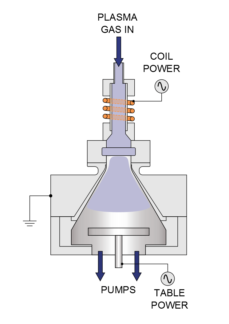
Atomic layer deposition technology (Atomic Layer Deposition, referred to as ALD) is a vacuum coating process that forms a thin film on the surface of a substrate layer by layer in the form of a single atomic layer. ALD technology is currently being widely adopted by the semiconductor industry.
Atomic layer deposition process:
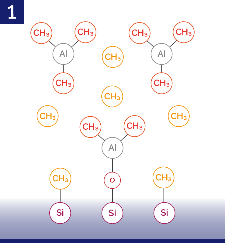
Atomic layer deposition usually includes a cycle of 4 steps, which is repeated as many times as needed to achieve the required deposition thickness. The following is an example of ALD of Al₂O₃, using precursor substances such as Al(CH₃) (TMA) and O₂.
Step 1) Add TMA precursor vapor to the substrate, TMA will adsorb on the substrate surface and react with it. By selecting appropriate precursor substances and parameters, the reaction will be self-limiting.
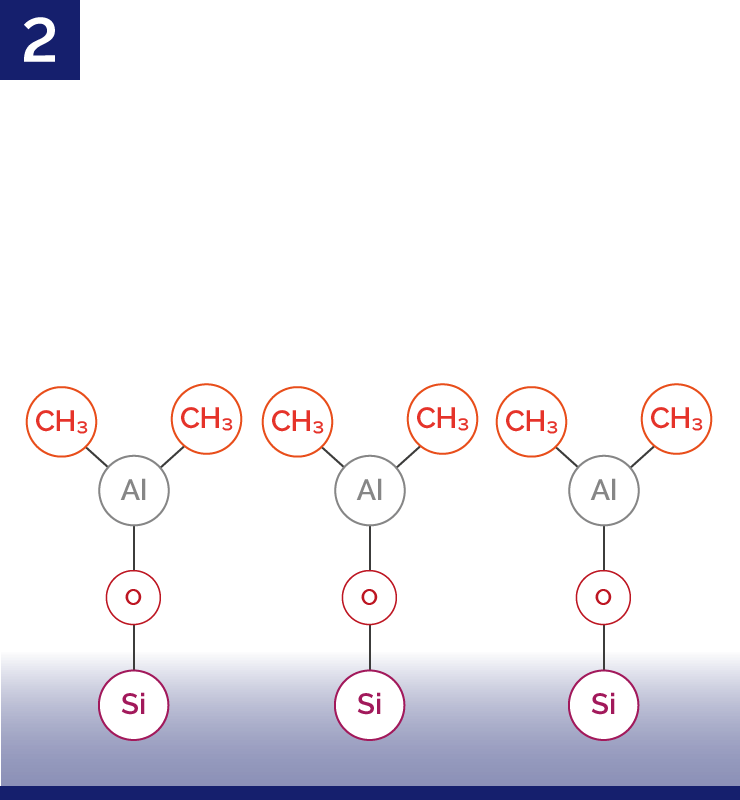
Step 2) Remove all residual precursors and reaction products.
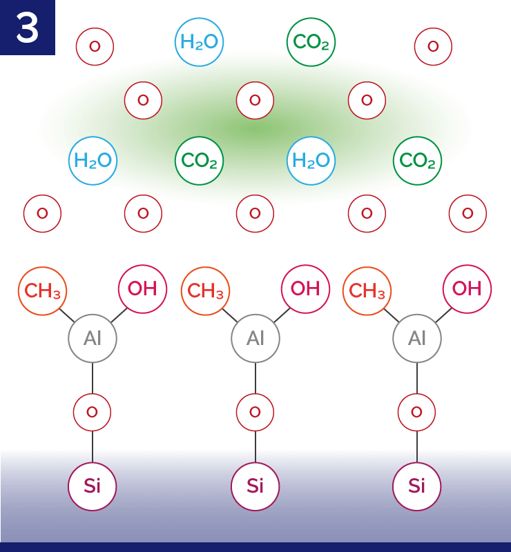
Step 3) Low-damage remote plasma irradiation of the surface with reactive oxygen radicals oxidizes the surface and removes surface ligands, a reaction that is also self-limiting due to the limited number of surface ligands.
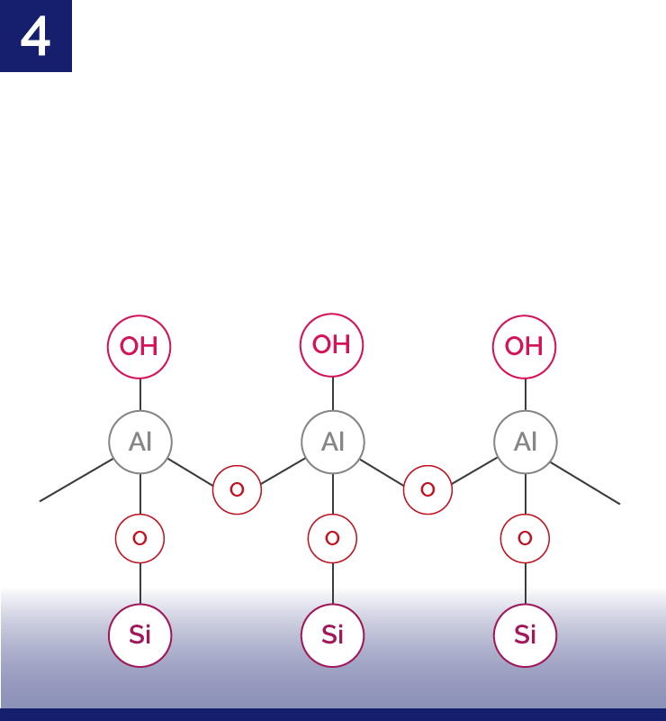
Step 4) Reaction products are removed from the chamber.
Only step 3 differs between thermal and plasma processes, with H₂O being used in thermal processes and O₂ plasma being used in plasma processes. Since the ALD process deposits (sub)-inch-thick films per cycle, the deposition process can be controlled at the atomic scale.
Highlights of Atomic Layer Deposition (ALD):
1) Grow high-quality thin films with extreme thickness accuracy, and only grow a single atomic layer at a time
2) Wafer thickness can reach 200 mm, with typical uniformity <±2%
3) Excellent step coverage even in high aspect ratio structures
4) Highly fitted coverage
5) Low pinhole and particle levels
6) Low damage and low temperature process
7) Reduce nucleation delay
8) Applicable to a variety of materials and processes
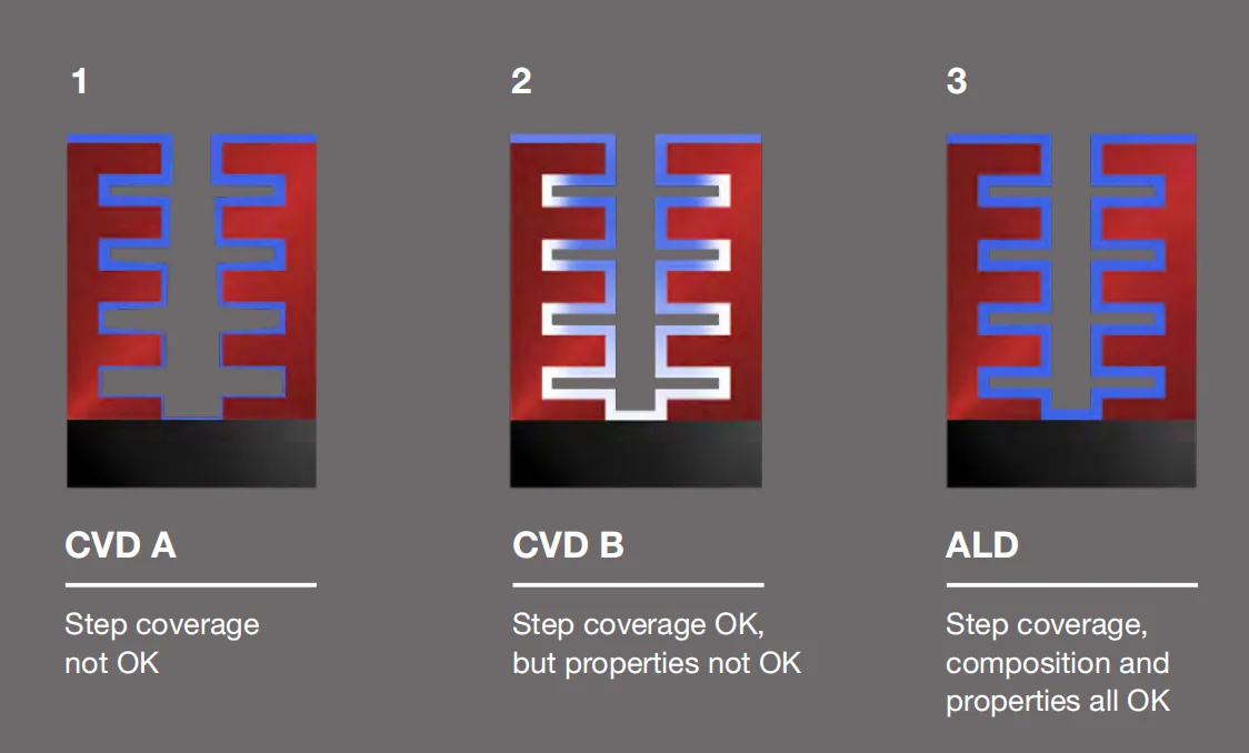
Compared with traditional chemical vapor deposition (CVD) and physical vapor deposition (PVD), the advantages of ALD are excellent three-dimensional conformality, large-area film uniformity, and precise thickness control, etc. It is suitable for growing ultra-thin films on complex surface shapes and high aspect ratio structures. Therefore, it is widely applicable to substrates of different shapes and does not require control of reactant flow uniformity.
Comparison of the advantages and disadvantages of PVD technology, CVD technology and ALD technology:
|
PVD technology |
CVD technology |
ALD technology |
|
Faster deposition rate |
Average deposition rate |
Slower deposition rate |
|
Thicker film thickness, poor control of nano-level film thickness precision |
Medium film thickness (depends on the number of reaction cycles) |
Atomic-level film thickness |
|
The coating has a single directionality |
The coating has a single directionality |
Good uniformity of large-area film thickness |
|
Poor thickness uniformity |
Average step coverage |
Best step coverage |
|
Poor step coverage |
\ |
Dense film without pinholes |
Advantages of ALD technology compared to CVD technology (Source: ASM)
Vetek Semiconductor is a professional ALD Susceptor products supplier in China. Our ALD Susceptor, SiC coating ALD susceptor and ALD Planetary Susceptor are widely used in key components of semiconductor manufacturing equipment. Vetek Semiconductor is committed to providing advanced and customizable ALD Susceptor products and technical solutions of various specifications for the semiconductor industry. We sincerely look forward to becoming your supplier in China.
- View as

گیرنده ALD
VeTek Semiconductor یک تولید کننده حرفه ای ALD Susceptor، پوشش CVD SiC، پایه گرافیت CVD TAC COATING در چین است. Vetek Semiconductor به طور مشترک پایه های سیاره ای ALD با پوشش SiC را با سازندگان سیستم ALD ایجاد و تولید کرد تا نیازهای بالای فرآیند ALD را برآورده کند و جریان هوا را به طور یکنواخت بر روی بستر توزیع کند. ما مشتاقانه منتظر همکاری بیشتر با شما هستیم.
ادامه مطلبارسال استعلام
گیرنده ALD پوشش SiC
به عنوان یک تولید کننده و تامین کننده حرفه ای گیرنده ALD پوشش SiC در چین، پوشش SiC نیمه هادی VeTek susceptor ALD یک جزء پشتیبانی است که به طور خاص در فرآیند رسوب لایه اتمی (ALD) استفاده می شود. این نقش کلیدی در تجهیزات ALD ایفا می کند و از یکنواختی و دقت فرآیند رسوب اطمینان می دهد. ما معتقدیم که محصولات ALD Planetary Susceptor ما می توانند راه حل های محصولی با کیفیت بالا را به شما ارائه دهند.
ادامه مطلبارسال استعلام
گیرنده سیاره ای ALD
فرآیند ALD، به معنای فرآیند اپیتاکسی لایه اتمی است. سازندگان سیستم های نیمه هادی Vetek و سیستم های ALD، گیرنده های سیاره ای ALD با پوشش SiC را توسعه داده و تولید کرده اند که الزامات بالای فرآیند ALD را برآورده می کند تا جریان هوا را به طور یکنواخت بر روی بستر توزیع کند. در عین حال، روکش CVD SiC با خلوص بالا Vetek Semiconductor خلوص را در این فرآیند تضمین می کند. به بحث در مورد همکاری با ما خوش آمدید.
ادامه مطلبارسال استعلام
به عنوان یک تولید کننده و تامین کننده حرفه ای ALD در چین، ما کارخانه خود را داریم. چه به خدمات سفارشیسازی شده برای رفع نیازهای خاص منطقه خود نیاز داشته باشید یا بخواهید پیشرفته و بادوام ALD ساخت چین بخرید، میتوانید برای ما پیام بگذارید.