- English
- Español
- Português
- русский
- Français
- 日本語
- Deutsch
- tiếng Việt
- Italiano
- Nederlands
- ภาษาไทย
- Polski
- 한국어
- Svenska
- magyar
- Malay
- বাংলা ভাষার
- Dansk
- Suomi
- हिन्दी
- Pilipino
- Türkçe
- Gaeilge
- العربية
- Indonesia
- Norsk
- تمل
- český
- ελληνικά
- український
- Javanese
- فارسی
- தமிழ்
- తెలుగు
- नेपाली
- Burmese
- български
- ລາວ
- Latine
- Қазақша
- Euskal
- Azərbaycan
- Slovenský jazyk
- Македонски
- Lietuvos
- Eesti Keel
- Română
- Slovenski
- मराठी
- Srpski језик


 coating")

ویفر
ویفر
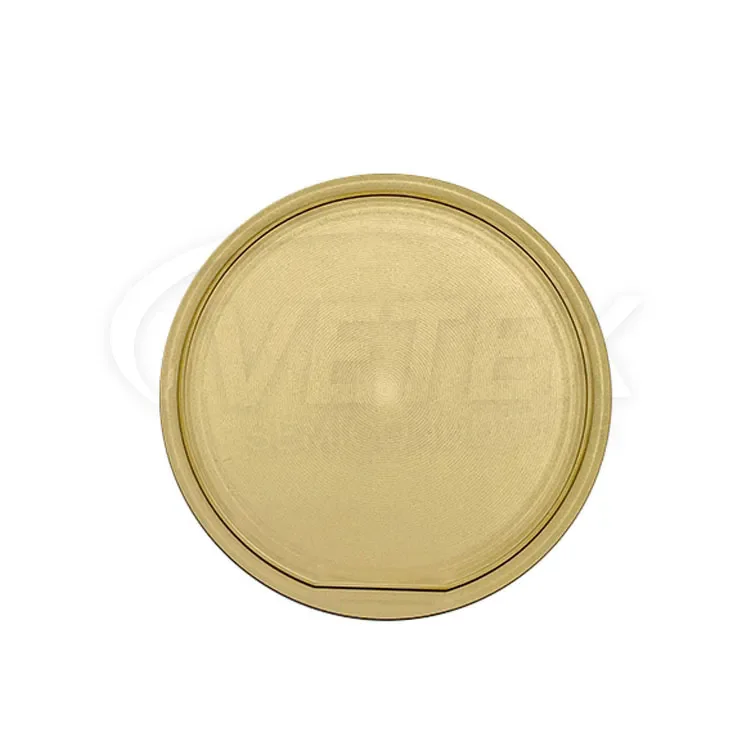
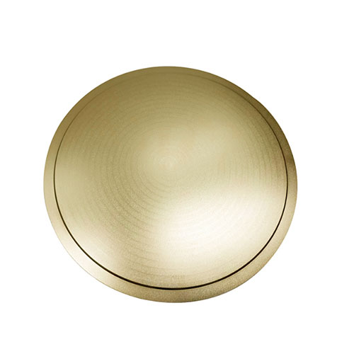
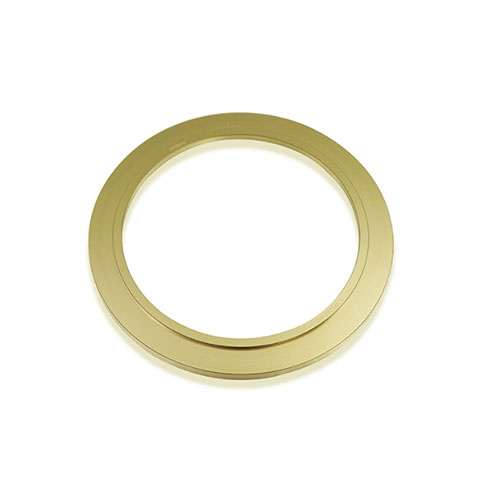
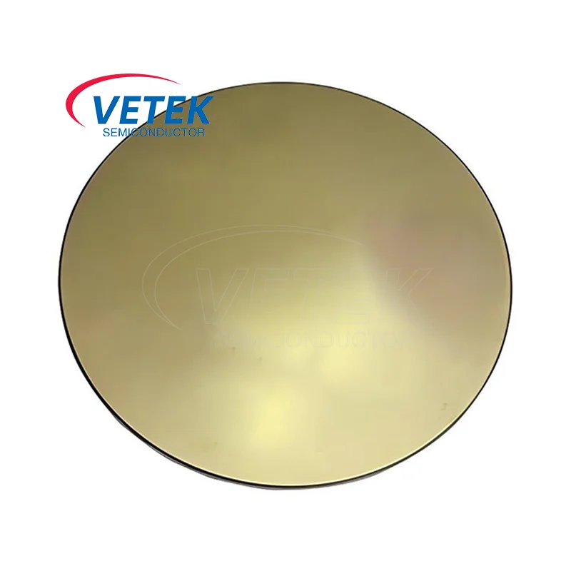
بستر ویفرویفر ساخته شده از مواد نیمه هادی تک کریستال است. بستر میتواند مستقیماً وارد فرآیند تولید ویفر برای تولید دستگاههای نیمهرسانا شود، یا میتوان آن را با فرآیند همبستگی برای تولید ویفرهای همپایه پردازش کرد.
بستر ویفر به عنوان ساختار اصلی حمایت کننده دستگاه های نیمه هادی، به طور مستقیم بر عملکرد و پایداری دستگاه ها تأثیر می گذارد. به عنوان "پایه" برای ساخت دستگاه های نیمه هادی، یک سری از فرآیندهای تولید مانند رشد لایه نازک و لیتوگرافی باید روی بستر انجام شود.
خلاصه ای از انواع بستر:
●ویفر سیلیکونی تک کریستال: در حال حاضر رایج ترین ماده زیرلایه است که به طور گسترده در ساخت مدارهای مجتمع (IC)، ریزپردازنده ها، حافظه ها، دستگاه های MEMS، دستگاه های قدرت و غیره استفاده می شود.
●بستر SOI: برای مدارهای مجتمع با کارایی بالا و کم مصرف، مانند مدارهای آنالوگ و دیجیتال با فرکانس بالا، دستگاه های RF و تراشه های مدیریت انرژی استفاده می شود.

●بسترهای نیمه هادی مرکب: بستر آرسنید گالیم (GaAs): دستگاه های ارتباطی امواج مایکروویو و میلی متری و ... بستر نیترید گالیوم (GaN): برای تقویت کننده های قدرت RF، HEMT و غیره استفاده می شود.بستر کاربید سیلیکون (SiC): برای وسایل نقلیه الکتریکی، مبدل های قدرت و سایر دستگاه های قدرت استفاده می شود.

●بستر یاقوت کبود: برای تولید LED، RFIC (مدار مجتمع فرکانس رادیویی) و غیره استفاده می شود.
Vetek Semiconductor یک تامین کننده حرفه ای زیرلایه SiC و بستر SOI در چین است. مازیرلایه SiC از نوع نیمه عایق 4Hو4H نیمه عایق نوع SiC بستربه طور گسترده در اجزای کلیدی تجهیزات تولید نیمه هادی استفاده می شود.
نیمه هادی وتک متعهد به ارائه محصولات پیشرفته و قابل تنظیم بستر ویفر و راه حل های فنی با مشخصات مختلف برای صنعت نیمه هادی است. ما صمیمانه منتظر تبدیل شدن به تامین کننده شما در چین هستیم.
ALD
ALD
Thin film preparation processes can be divided into two categories according to their film forming methods: physical vapor deposition (PVD) and chemical vapor deposition (CVD), of which CVD process equipment accounts for a higher proportion. Atomic layer deposition (ALD) is one of the chemical vapor deposition (CVD).
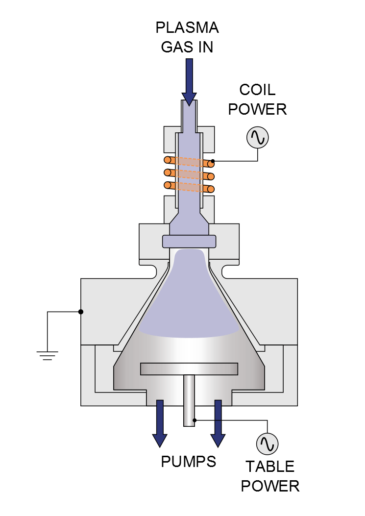
Atomic layer deposition technology (Atomic Layer Deposition, referred to as ALD) is a vacuum coating process that forms a thin film on the surface of a substrate layer by layer in the form of a single atomic layer. ALD technology is currently being widely adopted by the semiconductor industry.
Atomic layer deposition process:
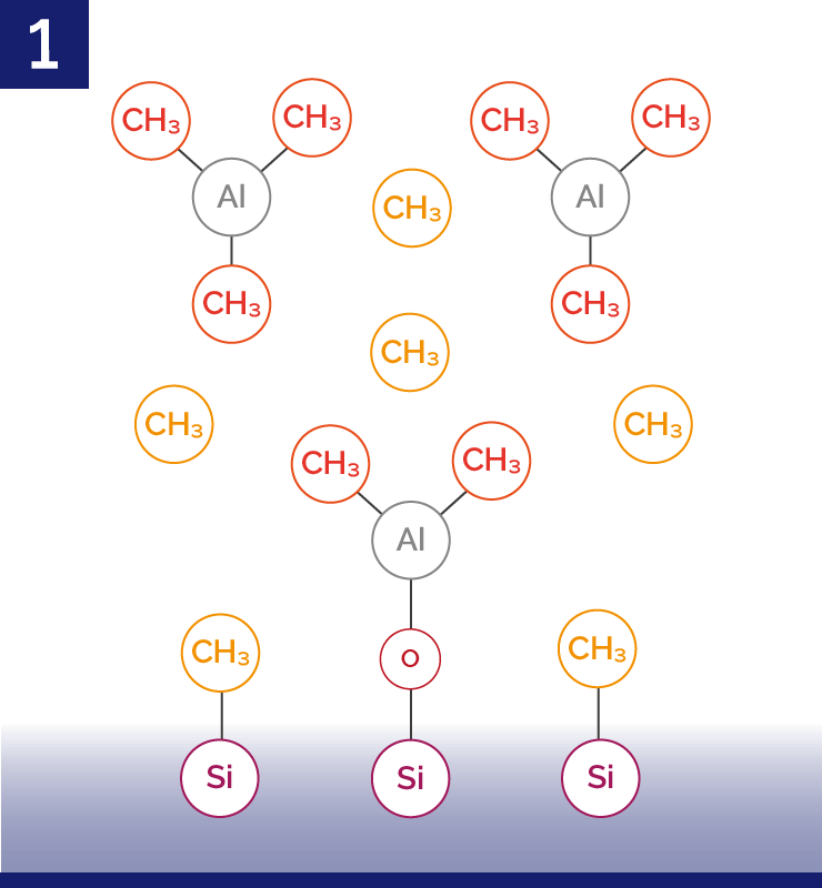
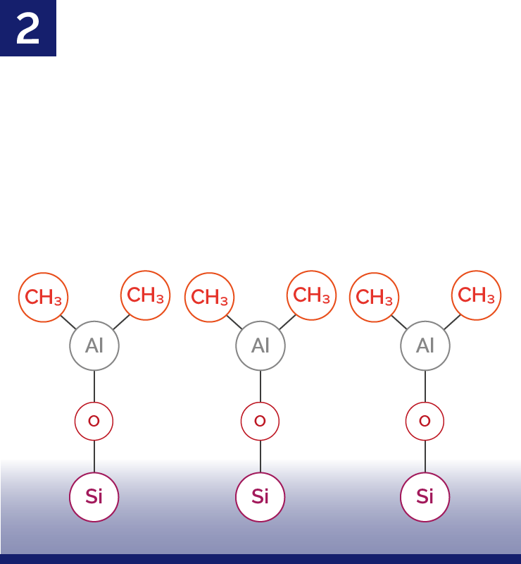
Atomic layer deposition usually includes a cycle of 4 steps, which is repeated as many times as needed to achieve the required deposition thickness. The following is an example of ALD of Al₂O₃, using precursor substances such as Al(CH₃) (TMA) and O₂.
Step 1) Add TMA precursor vapor to the substrate, TMA will adsorb on the substrate surface and react with it. By selecting appropriate precursor substances and parameters, the reaction will be self-limiting.
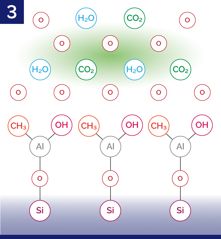
Step 2) Remove all residual precursors and reaction products.
Step 3) Low-damage remote plasma irradiation of the surface with reactive oxygen radicals oxidizes the surface and removes surface ligands, a reaction that is also self-limiting due to the limited number of surface ligands.
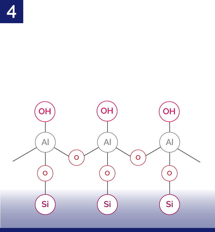
Step 4) Reaction products are removed from the chamber.
Only step 3 differs between thermal and plasma processes, with H₂O being used in thermal processes and O₂ plasma being used in plasma processes. Since the ALD process deposits (sub)-inch-thick films per cycle, the deposition process can be controlled at the atomic scale.
Highlights of Atomic Layer Deposition (ALD):
1) Grow high-quality thin films with extreme thickness accuracy, and only grow a single atomic layer at a time
2) Wafer thickness can reach 200 mm, with typical uniformity <±2%
3) Excellent step coverage even in high aspect ratio structures
4) Highly fitted coverage
5) Low pinhole and particle levels
6) Low damage and low temperature process
7) Reduce nucleation delay
8) Applicable to a variety of materials and processes
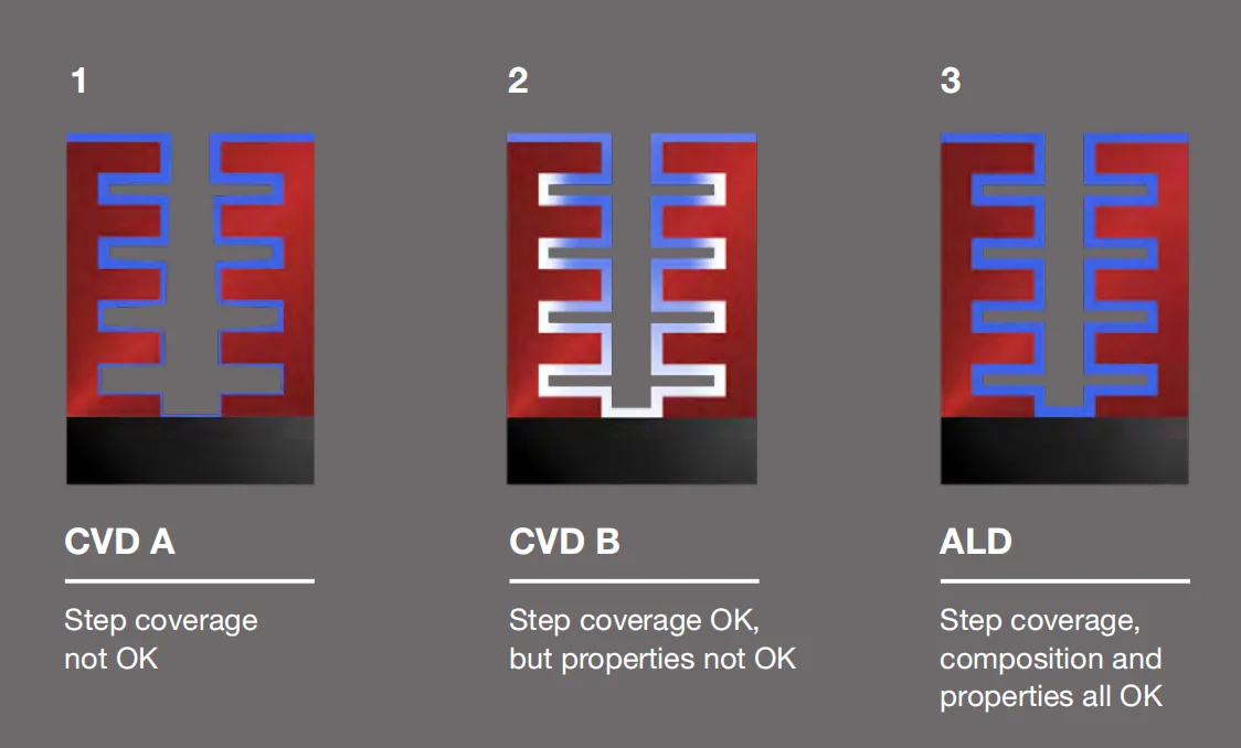
Compared with traditional chemical vapor deposition (CVD) and physical vapor deposition (PVD), the advantages of ALD are excellent three-dimensional conformality, large-area film uniformity, and precise thickness control, etc. It is suitable for growing ultra-thin films on complex surface shapes and high aspect ratio structures. Therefore, it is widely applicable to substrates of different shapes and does not require control of reactant flow uniformity.
Comparison of the advantages and disadvantages of PVD technology, CVD technology and ALD technology:
|
PVD technology |
CVD technology |
ALD technology |
|
Faster deposition rate |
Average deposition rate |
Slower deposition rate |
|
Thicker film thickness, poor control of nano-level film thickness precision |
Medium film thickness (depends on the number of reaction cycles) |
Atomic-level film thickness |
|
The coating has a single directionality |
The coating has a single directionality |
Good uniformity of large-area film thickness |
|
Poor thickness uniformity |
Average step coverage |
Best step coverage |
|
Poor step coverage |
\ |
Dense film without pinholes |
Advantages of ALD technology compared to CVD technology (Source: ASM)
Vetek Semiconductor is a professional ALD Susceptor products supplier in China. Our ALD Susceptor, SiC coating ALD susceptor and ALD Planetary Susceptor are widely used in key components of semiconductor manufacturing equipment. Vetek Semiconductor is committed to providing advanced and customizable ALD Susceptor products and technical solutions of various specifications for the semiconductor industry. We sincerely look forward to becoming your supplier in China.
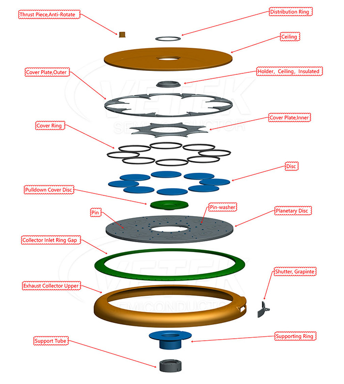
محصولات ویژه
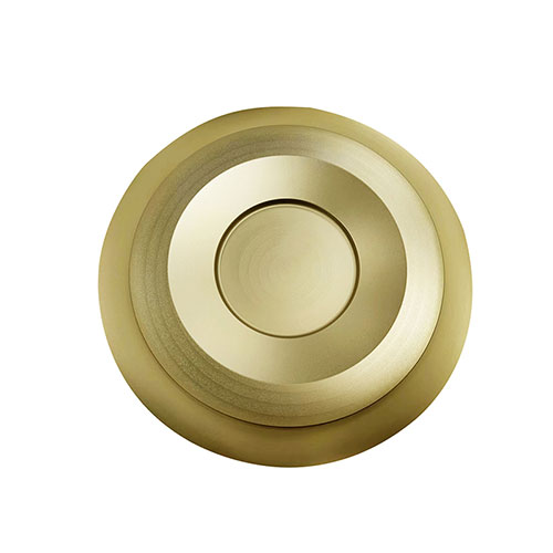
پوشش ماهواره ای با پوشش SiC برای MOCVD
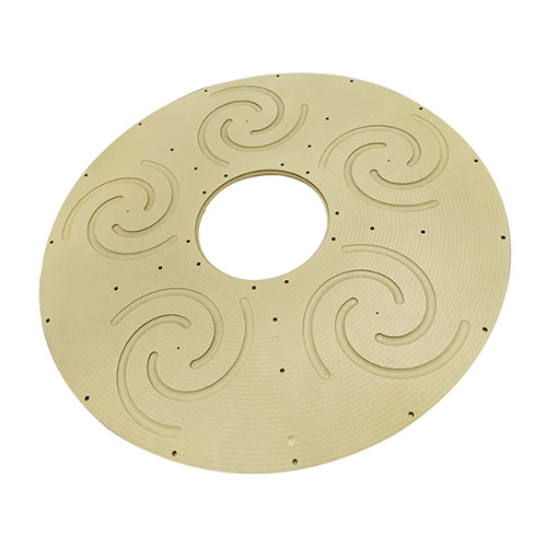
سر دوش دیسکی شکل جامد SiC
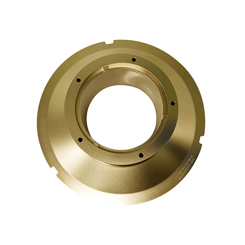
چاک الکترواستاتیک سرامیکی
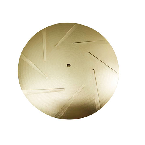
نگهدارنده بشکه ای ویفر با روکش CVD SiC
گیرنده بشکه پوشش سی سی سی
CVD SiC پوشش دهنده ویفر Epi Susceptor
نمد سخت گرافیت فوق خالص
لوله نمدی صلب با خلوص بالا
گیرنده گرافیت پوشش CVD SiC
عنصر گرمایش پوشش CVD SiC
گیرنده چرخان گرافیت
حلقه گرافیتی با خلوص بالا


درباره ما
VeTek Semiconductor Technology Co., LTD که در سال 2016 تأسیس شد، ارائه دهنده پیشرو مواد پوشش پیشرفته برای صنعت نیمه هادی است. بنیانگذار ما، کارشناس سابق موسسه مواد آکادمی علوم چین، این شرکت را با تمرکز بر توسعه راه حل های پیشرفته برای صنعت تاسیس کرد.
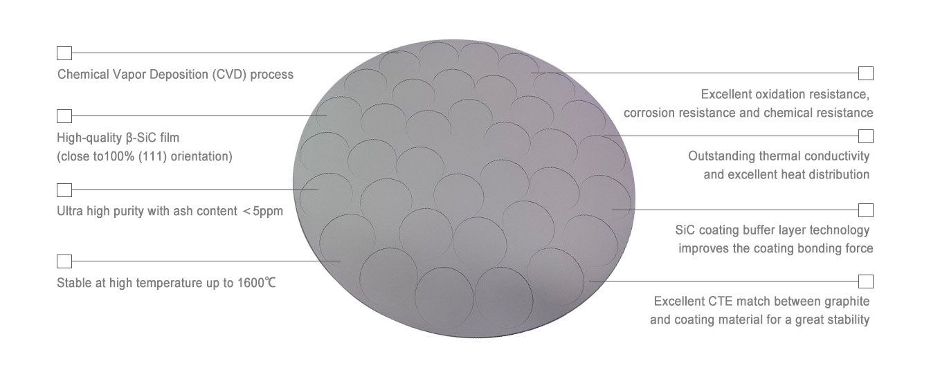
محصولات اصلی ما شاملپوشش های کاربید سیلیکون (SiC) CVD, پوشش های کاربید تانتالیوم (TaC), SiC فله، پودرهای SiC و مواد SiC با خلوص بالا. محصولات اصلی شامل گیرنده گرافیت با پوشش SiC، حلقه های پیش گرم، حلقه انحراف با پوشش TaC، قطعات نیمه ماه و غیره است، خلوص زیر 5ppm است، می تواند نیازهای مشتری را برآورده کند.
محصولات اصلی ما شاملپوشش های کاربید سیلیکون (SiC) CVD, پوشش های کاربید تانتالیوم (TaC), SiC فله، پودرهای SiC و مواد SiC با خلوص بالا. محصولات اصلی شامل گیرنده گرافیت با پوشش SiC، حلقه های پیش گرم، حلقه انحراف با پوشش TaC، قطعات نیمه ماه و غیره است، خلوص زیر 5ppm است، می تواند نیازهای مشتری را برآورده کند.

محصولات جدید
اخبار

فرآیند نیمه هادی: رسوب بخار شیمیایی (CVD)
رسوب بخار شیمیایی (CVD) در ساخت نیمه هادی ها برای رسوب مواد لایه نازک در محفظه از جمله SiO2، SiN و غیره استفاده می شود و از انواع معمول استفاده می شود PECVD و LPCVD. با تنظیم دما، فشار و نوع گاز واکنش، CVD به خلوص بالا، یکنواختی و پوشش خوب فیلم برای برآوردن نیازهای فرآیند مختلف دست می یابد.
ادامه مطلب

چگونه مشکل زینترینگ ترک در سرامیک های کاربید سیلیکون را حل کنیم؟ - نیمه هادی VeTek
این مقاله عمدتاً چشم انداز کاربرد گسترده سرامیک های کاربید سیلیکون را توصیف می کند. همچنین بر تجزیه و تحلیل علل ترک های تف جوشی در سرامیک های کاربید سیلیکون و راه حل های مربوطه تمرکز دارد.
ادامه مطلب

رشد اپیتاکسیال با کنترل مرحله ای چیست؟
ادامه مطلب

مشکلات در فرآیند اچینگ
فناوری اچینگ در تولید نیمه هادی اغلب با مشکلاتی مانند اثر بارگذاری، اثر میکرو شیار و اثر شارژ مواجه می شود که بر کیفیت محصول تأثیر می گذارد. راه حل های بهبود عبارتند از بهینه سازی چگالی پلاسما، تنظیم ترکیب گاز واکنش، بهبود کارایی سیستم خلاء، طراحی طرح لیتوگرافی معقول، و انتخاب مواد ماسک اچینگ مناسب و شرایط فرآیند.
ادامه مطلب

سرامیک داغ SiC چیست؟
تف جوشی پرس گرم روش اصلی برای تهیه سرامیک های SiC با کارایی بالا است. فرآیند تف جوشی پرس گرم شامل: انتخاب پودر SiC با خلوص بالا، پرس و قالب گیری در دمای بالا و فشار بالا و سپس تف جوشی است. سرامیک های SiC تهیه شده با این روش دارای مزایای خلوص بالا و چگالی بالا هستند و به طور گسترده در سنگ زنی دیسک ها و تجهیزات عملیات حرارتی برای پردازش ویفر استفاده می شوند.
ادامه مطلب

کاربرد مواد میدان حرارتی مبتنی بر کربن در رشد کریستال کاربید سیلیکون
روشهای رشد کلیدی کاربید سیلیکون (SiC) شامل PVT، TSSG و HTCVD است که هر کدام مزایا و چالشهای متمایزی دارند. مواد میدان حرارتی مبتنی بر کربن مانند سیستمهای عایق، بوتهها، پوششهای TaC و گرافیت متخلخل با ایجاد ثبات، هدایت حرارتی و خلوص، رشد کریستال را افزایش میدهند که برای ساخت و کاربرد دقیق SiC ضروری است.
ادامه مطلب